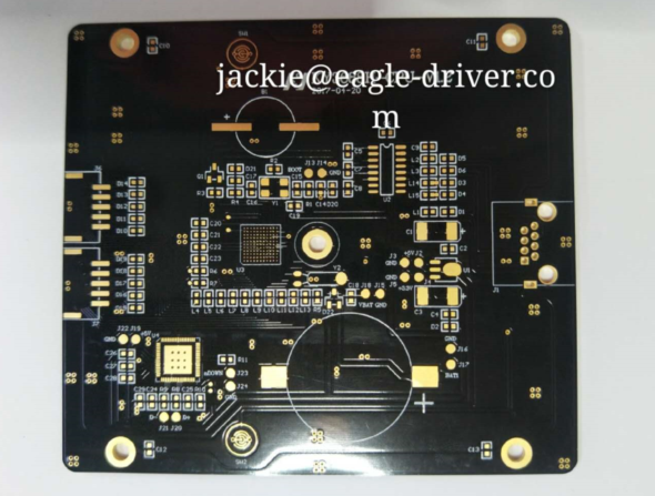


The PCB is designed to be
smaller, faster and cheaper.As the interconnection point is the weakest link in
the circuit chain, the electromagnetic property at the interconnection point is
the main problem faced by the engineering design in the RF design. Every
interconnection point should be investigated and the existing problems solved.
Interconnection of PCB system
includes chip to PCB, interconnection of PCB board and signal input/output
between PCB and external device.This paper mainly introduces the practical
summary of high frequency PCB design by interconnection in PCB board. It is
believed that the understanding of this paper will bring convenience to PCB
design in the future.
Interconnection between chip
and PCB is important in PCB design. However, the main problem of
interconnection between chip and PCB is that too high interconnection density
will lead to the basic structure of PCB materials becoming a factor limiting
the growth of interconnection density.This article shares the practical
techniques of high frequency PCB design.For high frequency applications, the
following techniques are used to design high frequency PCB with interconnection
in PCB boards:

1, the transmission line to the corner a 45 ° Angle, in order to
reduce return loss;
2. High performance insulation
circuit board shall be strictly controlled by insulation constant value
according to hierarchy.This method is beneficial to the effective management of
the electromagnetic field between the insulating material and the adjacent
wiring.
3. Improve the PCB design
specifications for high precision etching.Consider setting the total line width
error to +/-0.0007 inches, managing undercut and cross sections of the wire
shape, and specifying the conditions for side wall plating of the wire.The
overall management of the geometry and coating surfaces of wiring (wires) is
very important for solving the skin effect related to microwave frequency and
realizing these specifications.
4. Highlight the presence of
tap inductor in the lead, and avoid the use of components with lead.In high
frequency environments, it is best to use surface mounted components.
5. For signal perforation,
avoid using PTH process on sensitive plate.Because this process will lead to
lead inductance at the hole.For example, when a hole in a 20-layer plate is
used to connect 1 to 3 layers, the lead inductor can affect 4 to 19 layers.
6. Provide a rich seam
connection.A die hole is used to connect these layers together to prevent the
impact of a 3-dimensional electromagnetic field on the circuit board.
7. To choose non-electrolytic
nickel plating or dip plating process, do not use HASL method for plating.This
electroplating surface can provide a better skin effect for high frequency
current.In addition, the high solderable coating requires less lead wire and
helps reduce environmental pollution.
8. The welding resistance layer
can prevent the soldering paste from flowing.However, due to the uncertainty of
thickness and the uncertainty of insulation performance, covering the entire
plate surface with welding resistance materials will lead to a large change in
electromagnetic energy in microstrip design.Solderdam is commonly used as the
resistance layer.
·
EAGLE DRIVER ELECTRONIC LIMITED--Outstanding
in PCB production.


